
Micron to bond wafers for G11 NAND launch in late 2027
The new memory chip doubles density to 42 Gb/mm2 and boosts I/O speed by 50 percent.
By Nicholas Martin ·
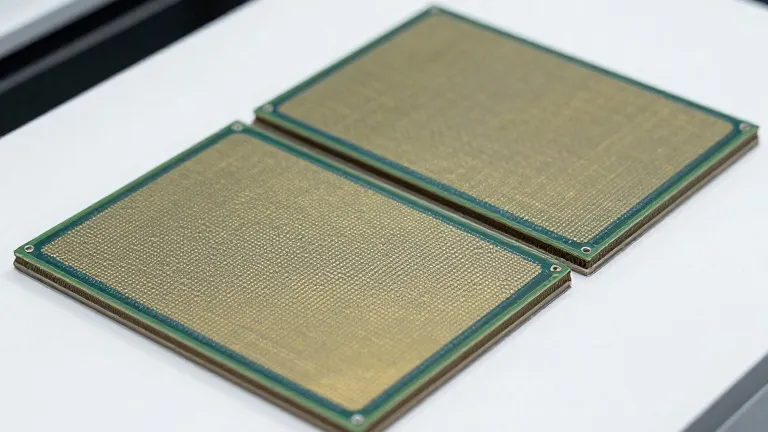
Micron detailed its next generation of 3D NAND flash storage on Thursday.
The company, which calls the product G11, plans to begin high-volume production in the second half of 2027. Micron stated that the new chip will offer roughly twice the storage density of its current G9 generation. The G9 chip operates at approximately 21 Gb/mm2 in triple-level-cell form. G11 will reach 42 Gb/mm2.
Performance metrics also improve. I/O speeds will rise from 3,600 MT/s to 5,400 MT/s. That represents a 50 percent increase. Energy consumption for data transfer will drop by more than 25 percent. These specifications exceed the next-generation products from competitors Kioxia and Samsung.
Scott DeBoer, Micron's president and chief technology and products officer, presented the roadmap at a recent industry event. He confirmed that G11 relies on wafer-on-wafer bonding. DeBoer described the timing as right for the technology and labeled G11 the world's most advanced NAND. Micron previously used CMOS-under-array designs. The bonding method allows engineers to build the memory array and the peripheral circuitry on separate wafers. Each wafer uses a manufacturing process optimized for its specific function. The two wafers are then bonded together.
The G11 architecture will feature more than 400 layers. Micron did not disclose the exact number of active wordline layers or memory decks. The company said the design will have an industry-leading memory cell pitch. This suggests the density gain comes from both additional layers and smaller cell dimensions. Micron will share more technical details in 2027 as production starts.
The new chips target high-capacity SSDs for clients and data centers. They also address storage devices built for artificial intelligence workloads. These applications require higher bandwidth and better energy efficiency. DeBoer said the company will continue scaling in all three dimensions beyond G11. He mentioned developing high-mobility materials and ultra-dense cell architectures. These future improvements aim to cut energy usage and allow for smaller cells.
Micron has not released specific targets for generations following G11. The company said it would not go into great detail on the long-term roadmap today. Both the industry and Micron continue to scale by adding layers and shrinking cell dimensions.
Source: Tom's Hardware